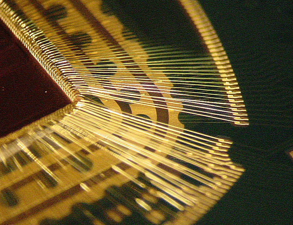
IC
Repackaging
In the field of failure analysis
and device characterization, it is often useful for assembling
of a device into another secondary package. With the advancement
of semiconductor process and package, failure analysis and
device characterization techniques such as (photoemission
microscopy analysis, FIB, EMISCOPE, LIVA, TIVA, OBIRCH,
etc.) from the top side of the die can be difficult. Analysis
from the backside of the die has become an alternate technique.
IC repackaging allows analysis from the backside of the
die without required expensive modification of hardware
and test programs. IC repackaging often requires all or
some the following steps:
- Backside thinning of the
device to 150um or less.
- Polish the package substrate of the
device to expose the bondwire of the device.
- Preparation of the sencondary package
substrate.
- Remap the bonding to meet the new mount
and bond diagram.
- Attached a device to the new package
substrate.
- Bond the required pins.
- Encapsulate (Glop)
|


